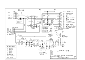
Start with making a paper copy of this diagram. This is a large version that can be printed on a A4 sheet.
The GPS interface can be fed in 2 ways: with a stabilized 5V supply or with a 10 to 25V unregulated DC supply. In both cases the power is fed into the RJ45 connector on point 8. Pin 7 is DC ground.
The power supply current is first secured with a slow 315mA fuse (in socket). Then there is a Transzorb device to ground. This device is a short-circuit for reverse polarity voltages and for voltages above 27V. It causes the fuse to blow and in doing so, protecting the other electronics and GPS module.
After the Transzorb there are several other components for filtering and the unregulated voltage is supplied to the switching regulator U2. This LT1107CN8-5 (datasheet) produces 5V without much heat losses. A linear regulator like a 7805 would dissipate approx. 2 Watts. With this switching regulator the dissipation is limited to max. 0,3Watts. R10 defines the output voltage. If it is 0 ohm, the output voltage would be exactly 5V. We chose to make it 5k6 ohm so the output voltage becomes approx. 5,1V. This is done to compensate for the loss in the filter around L3. R9 is only used when you use the adjustable version of the LT1107, and since we supply the fixed 5V output version, this position stays unpopulated.
The regulated 5V is then wired to the 2-position jumper SW5. With this jumper we can choose between the 5V from the LT1107 regulator (position 2), or from an externally supplied 5V regulated supply (position 1). After this jumper ther is an additional Transzorb to ground. This one short-circuits everything above 6V. If the SW5 jumper is in position 1 (external 5V) and a higher voltage is supplied, this Transzorb burns the fuse end protects the sensitive GPS module.
After some more filtering (C6, L3, C7, C8) the +5V is offered to the GPS module and the RS232 converter. There is also a simple charging circuit consisting of D6, D7 and R6 for an optional NiCd battery to keep the real-time clock and static ram of the GPS module powered, as to speed up locking to the GPS constellation after power-up. However, we chose to not deliver this NiCd battery and instead offer a 0,22F 5,5V supercap, that can be soldered directly onto the GPS module. This supercap keeps the clock running for approx. 2 days. If you want longer retention you will have to mount a 3,6V NiCd PCB-mount battery, for example the Emmerich NC-M120-3,6V type, or any other 3,6V NiCd or NiMH type. You can also choose to use a non-recharable 3V Lithium cel. In that case, do not mount the charging circuit or disconnect it from the battery.
Via jumper SW4 and a 10 ohm series resistor R7 5V is offered to the GPS module to feed an external active antenna. When you use a passive antenna, leave SW4 open.
The GPS module outputs a serial TTL (0V / 5V) signal. This must be converted to RS232 levels (+5 to 15 / -5 to 15V) before it is usable by the PC host computer.
The RS232 level convertor is the conventional circuit around a MAX232 (U1). The 4 converters in this chip are all used: 2 for the NMEA serial data input and output port, 1 output to convert the 1PPS signal to RS232 levels and 1 input for connecting an optional differential GPS receiver.
The 1PPS signal can be connected to either pin 1 (DCD), pin 6 (DSR) or pin 8 (CTS) of the serial port.
Software like NMEAtime or Linux time server can use this 1PPS signal to achieve a a very accurate time synchronisation. Every software package has its own way of detecting this 1PPS signal, and some softeware packages don't use it al all. Therefore the 1PPS signal is configurable on pin 1, 6 or 8 of the DB9 connector. If the software you use does not make use of this option, than don't wire anything at all.
The DB9 connector is wired as a modem. If you have an existing modem cable it can be used to connect the GPS kit to the serial port of the PC or laptop.
All signals are also wired to the RJ45 connector, so the DB9 female PCB connector is in fact optional when filling the PCB with components. However, you will need to make your own cable.
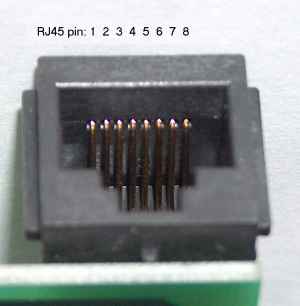
For the power supply and variuous other signals a RJ45 connector with 8 contacts has been chosen. This is a much-used and robust connector. The disadvantage is that you need a special crimping tool and special cable tou correctly mount a cable. These tools are available for prices of around 10-15 Euro. For a small fee we can supply you with some cables that enable you to make your own cable. But you can also buy a UTP network cable at the local PC shop. Make sure you buy a network cable with all 8 contacts wired!
The pinout:
| contact | direction | level | description. |
| pin 1 | output | RS232 | 1 PPS signal on RS232 level. Locked on GPS timebase. |
| pin 2 | output | RS232 | NMEA data port output.. |
| pin 3 | input | RS232 | NMEA data port input. |
| pin 4 | output | TTL | 10kHz squarewave locked on GPS timebase. |
| pin 5 | input | RS232 | 2nd serial port for optional differential GPS receiver. |
| pin 6 | output | TTL | 1PPS signal on TTL levels, directly from GPS module. locked on GPS timebase. |
| pin 7 | ground | 0 Volt | common, for both the RS232 port and for the power supply. |
| pin 8 | power | +5 or +10..+25V | depending on the position of jumper SW5. |
The TTL signals are directly connected to the GPS module.
| Jumper | function | position | position | remark |
| SW1 | RESET | 1=reset active | 2=normal | pin 5 GPS module |
| SW2 | boot mode NMEA mode | 1=start in NMEA mode | 2=start determined by SW3 | pin 7 GPS module |
| SW3 | boot mode ROM defaults | 1=start from ROM default parameters |
2=start parameters from Sram/EEprom |
pin 8 GPS module |
| SW4 | Antenna supply | jumper on = 5V active antenna | jumper off = passive antenna | pin 1 GPS module |
| SW5 | input power selection | 1=5V regulated | 2=10 to 28V unregulated | |
| PS-1/6/8 | 1PPS rs232 output selection | wire PS-1 = 1PPS on CD wire PS-6 = 1PPS on DSR wire PS-8 = 1PPS on CTS |
see remark |